- 您现在的位置:买卖IC网 > Sheet目录3862 > PIC18F45J11-I/ML (Microchip Technology)IC PIC MCU FLASH 32K 2V 44-QFN
2010
Micr
ochip
T
e
ch
nol
ogy
I
n
c.
DS7
0138G
-page
89
dsPIC30F3014/4
013
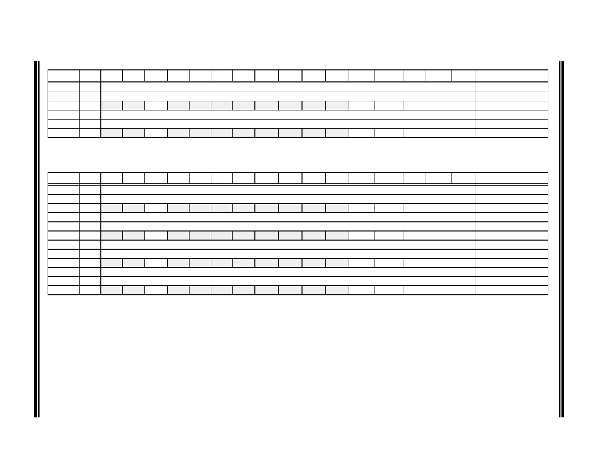
TABLE 13-1:
dsPIC30F3014 OUTPUT COMPARE REGISTER MAP(1)
TABLE 13-2:
dsPIC30F4013 OUTPUT COMPARE REGISTER MAP(1)
SFR Name
Addr.
Bit 15
Bit 14
Bit 13
Bit 12
Bit 11
Bit 10
Bit 9
Bit 8
Bit 7
Bit 6
Bit 5
Bit 4
Bit 3
Bit 2
Bit 1
Bit 0
Reset State
OC1RS
0180
Output Compare 1 Secondary Register
0000 0000 0000 0000
OC1R
0182
Output Compare 1 Main Register
0000 0000 0000 0000
OC1CON
0184
—
—OCSIDL
—
OCFLT
OCTSEL
OCM<2:0>
0000 0000 0000 0000
OC2RS
0186
Output Compare 2 Secondary Register
0000 0000 0000 0000
OC2R
0188
Output Compare 2 Main Register
0000 0000 0000 0000
OC2CON
018A
—
—OCSIDL
—
OCFLT
OCTSE
OCM<2:0>
0000 0000 0000 0000
Legend:
— = unimplemented bit, read as ‘0’
Note
1:
Refer to the “dsPIC30F Family Reference Manual” (DS70046) for descriptions of register bit fields.
SFR Name
Addr.
Bit 15
Bit 14
Bit 13
Bit 12
Bit 11
Bit 10
Bit 9
Bit 8
Bit 7
Bit 6
Bit 5
Bit 4
Bit 3
Bit 2
Bit 1
Bit 0
Reset State
OC1RS
0180
Output Compare 1 Secondary Register
0000 0000 0000 0000
OC1R
0182
Output Compare 1 Main Register
0000 0000 0000 0000
OC1CON
0184
—
—OCSIDL
—
OCFLT
OCTSEL
OCM<2:0>
0000 0000 0000 0000
OC2RS
0186
Output Compare 2 Secondary Register
0000 0000 0000 0000
OC2R
0188
Output Compare 2 Main Register
0000 0000 0000 0000
OC2CON
018A
—
—OCSIDL
—
OCFLT
OCTSE
OCM<2:0>
0000 0000 0000 0000
OC3RS
018C
Output Compare 3 Secondary Register
0000 0000 0000 0000
OC3R
018E
Output Compare 3 Main Register
0000 0000 0000 0000
OC3CON
0190
—
—OCSIDL
—
OCFLT
OCTSEL
OCM<2:0>
0000 0000 0000 0000
OC4RS
0192
Output Compare 4 Secondary Register
0000 0000 0000 0000
OC4R
0194
Output Compare 4 Main Register
0000 0000 0000 0000
OC4CON
0196
—
—OCSIDL
—
OCFLT
OCTSEL
OCM<2:0>
0000 0000 0000 0000
Legend:
— = unimplemented bit, read as ‘0’
Note
1:
Refer to the “dsPIC30F Family Reference Manual” (DS70046) for descriptions of register bit fields.
发布紧急采购,3分钟左右您将得到回复。
相关PDF资料
SFW15R-2STE1
SFW15R-2STE1-FFC/FPC CONN
PIC18F26J11-I/ML
IC PIC MCU FLASH 64K 2V 28-QFN
PIC18F46K20-E/ML
IC PIC MCU FLASH 32KX16 44QFN
PIC24FJ64GA002-I/SO
IC PIC MCU FLASH 64KB 28SOIC
PIC16C711-04/P
IC MCU OTP 1KX14 A/D 18DIP
PIC18LF26K22-I/SP
IC PIC MCU 64KB FLASH 28SPDIP
PIC18F25K80-I/SP
MCU PIC 32KB FLASH 28SDIP
DSPIC33FJ12MC201-I/SS
IC DSPIC MCU/DSP 12K 20SSOP
相关代理商/技术参数
PIC18F45J11-I/PT
功能描述:8位微控制器 -MCU 32KB Flash 4KBRAM 12MIPS nanoWatt RoHS:否 制造商:Silicon Labs 核心:8051 处理器系列:C8051F39x 数据总线宽度:8 bit 最大时钟频率:50 MHz 程序存储器大小:16 KB 数据 RAM 大小:1 KB 片上 ADC:Yes 工作电源电压:1.8 V to 3.6 V 工作温度范围:- 40 C to + 105 C 封装 / 箱体:QFN-20 安装风格:SMD/SMT
PIC18F45J11T-I/ML
功能描述:8位微控制器 -MCU 32KB Flash 4KBRAM 12MIPS nanoWatt RoHS:否 制造商:Silicon Labs 核心:8051 处理器系列:C8051F39x 数据总线宽度:8 bit 最大时钟频率:50 MHz 程序存储器大小:16 KB 数据 RAM 大小:1 KB 片上 ADC:Yes 工作电源电压:1.8 V to 3.6 V 工作温度范围:- 40 C to + 105 C 封装 / 箱体:QFN-20 安装风格:SMD/SMT
PIC18F45J11T-I/PT
功能描述:8位微控制器 -MCU 32KB Flash 4KBRAM 12MIPS nanoWatt RoHS:否 制造商:Silicon Labs 核心:8051 处理器系列:C8051F39x 数据总线宽度:8 bit 最大时钟频率:50 MHz 程序存储器大小:16 KB 数据 RAM 大小:1 KB 片上 ADC:Yes 工作电源电压:1.8 V to 3.6 V 工作温度范围:- 40 C to + 105 C 封装 / 箱体:QFN-20 安装风格:SMD/SMT
PIC18F45J50-I/ML
功能描述:8位微控制器 -MCU Full Spd USB 32KB 4KBRAM nanoWatt RoHS:否 制造商:Silicon Labs 核心:8051 处理器系列:C8051F39x 数据总线宽度:8 bit 最大时钟频率:50 MHz 程序存储器大小:16 KB 数据 RAM 大小:1 KB 片上 ADC:Yes 工作电源电压:1.8 V to 3.6 V 工作温度范围:- 40 C to + 105 C 封装 / 箱体:QFN-20 安装风格:SMD/SMT
PIC18F45J50-I/PT
功能描述:8位微控制器 -MCU Full Spd USB 32KB 4KBRAM nanoWatt
RoHS:否 制造商:Silicon Labs 核心:8051 处理器系列:C8051F39x 数据总线宽度:8 bit 最大时钟频率:50 MHz 程序存储器大小:16 KB 数据 RAM 大小:1 KB 片上 ADC:Yes 工作电源电压:1.8 V to 3.6 V 工作温度范围:- 40 C to + 105 C 封装 / 箱体:QFN-20 安装风格:SMD/SMT
PIC18F45J50T-I/ML
功能描述:8位微控制器 -MCU Full Spd USB 32KB 4KBRAM nanoWatt RoHS:否 制造商:Silicon Labs 核心:8051 处理器系列:C8051F39x 数据总线宽度:8 bit 最大时钟频率:50 MHz 程序存储器大小:16 KB 数据 RAM 大小:1 KB 片上 ADC:Yes 工作电源电压:1.8 V to 3.6 V 工作温度范围:- 40 C to + 105 C 封装 / 箱体:QFN-20 安装风格:SMD/SMT
PIC18F45J50T-I/PT
功能描述:8位微控制器 -MCU Full Spd USB 32KB 4KBRAM nanoWatt RoHS:否 制造商:Silicon Labs 核心:8051 处理器系列:C8051F39x 数据总线宽度:8 bit 最大时钟频率:50 MHz 程序存储器大小:16 KB 数据 RAM 大小:1 KB 片上 ADC:Yes 工作电源电压:1.8 V to 3.6 V 工作温度范围:- 40 C to + 105 C 封装 / 箱体:QFN-20 安装风格:SMD/SMT
PIC18F45K20-E/ML
功能描述:8位微控制器 -MCU 32KB Flash 1536B RAM 25 I/O 8B RoHS:否 制造商:Silicon Labs 核心:8051 处理器系列:C8051F39x 数据总线宽度:8 bit 最大时钟频率:50 MHz 程序存储器大小:16 KB 数据 RAM 大小:1 KB 片上 ADC:Yes 工作电源电压:1.8 V to 3.6 V 工作温度范围:- 40 C to + 105 C 封装 / 箱体:QFN-20 安装风格:SMD/SMT